Enabling a Digital Transformation of Advanced Additive Electronics
by Dave Wiens, Siemens EDA
In this piece, I’ll take a look at emerging technologies for additive manufacturing, but with the same goal: an optimized digital thread through design, verification, and manufacturing.
Additive manufacturing has been around electronics since thick-film, screened hybrids came on the scene more than 30 years ago. And while those never quite went away, they never gained the prominence we all expected alongside the more traditional laminated, subtractive-etched PCBs. Today, emerging technologies are bringing a resurgence in additive manufacturing, thanks to a host of new materials, machines, and processes.
Electronics have historically been discrete structures encapsulated in some mechanical package. The drive now is to integrate electronics more seamlessly into the end-product’s form factor, requiring circuits that are flexible and/or conformal to the contours of any product surface. In addition to reduced size and weight, other drivers include customization with localized manufacturing, reduction in part count, new 3D structures, and a reimagined supply chain.
There are a number of applications for this new technology, including radar systems and other sensors molded to the surface of an airplane, smart textiles with integrated sensors to measure human performance and provide identification, and medical bandages that sense infection and accelerate healing. Cars are rife with sensors across both the exterior and interior surfaces, conforming to the design of the car, not the other way around. Even product packaging includes sensors that track conditions during shipment to ensure quality.
Design for additive manufacturing
From the designer’s perspective, these technologies can be broken into planar and non-planar categories.
Planar electronics are designed with processes similar to those used for traditional, flat PCB-like layered structures. The manufacturing may be very different (e.g., using an additive printer), but it’s still creating the structure one planar layer at a time. Post-production, they can be flexed or molded into the final form. Advanced technologies that fit the planar design model today include flexible hybrid electronics (everything’s flexible, including the ICs and batteries), molded interconnects, and 3D conformal “wraps” (e.g., 2D designs converted to fit a 3D structure, then printed).
PCB design tool advances made over the years to support rigid-flex, localized dielectrics, HDI, wire bonding, and embedded actives/passives can aid in the design of planar structures (i.e., make the digital twin more intelligent, rather than creating workarounds that have to be explained or converted for manufacturing). Certainly, design for manufacturability takes on new meaning when you have to ensure things like interconnect and impedance continuity in the final flexed/conformal structure. In this design chain, MCAD tools become more critical, but there’s still the physical separation between electronics and associated mechanical enclosures or mounts.
Non-planar electronics can have interconnects and components placed at any angle, in any location in a given space. There’s no functional reason to separate electronics from a mechanical enclosure. They’re one and the same—the ultimate in electro-mechanical structures. Given the geometrical challenges, current prototypes of these structures are often designed in MCAD as non-electrically intelligent structures, forgoing much of the automation and verification technologies built up over decades in ECAD. These structures are still relatively simple, so the trade-off is acceptable, but as complexity increases, the need to maintain electrical intelligence and model performance will increase.
Optimizing the tool chain
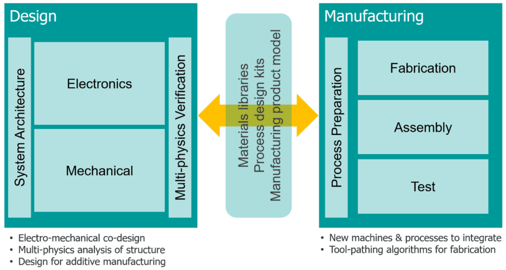
Over the last 50 plus years of PCB design and manufacturing, the tool chain from design through manufacturing has become fairly optimized (there are still areas for improvement). As noted in the introduction, the goal for additive manufacturing is to achieve the same optimizations, ensuring a continuous digital thread so that there is absolutely no redesign as the design passes through various design and verification tools and on through to manufacturing (see Figure1). Part of the challenge today is that there are so many manufacturing technologies and materials in research that it’s hard to focus on optimizing a moving target.

Figure 1: Tool chain for 3D printed electro-mechanical structures
At first glance, the process chart in Figure 1 could easily represent traditional PCB flows, but a closer look reveals many new challenges:
- The delineation between ECAD and MCAD is blurring so much that electro-mechanical design may have to be done in one tool.
- Design constraints will have to consider the variability of the materials used.
- Given the operating conditions of these new structures, a host of multi-physics analysis will be required to ensure performance (e.g., signal, power, thermal, EMI, stress, vibration, stretch, moisture, impact, deformation, and manufacturability).
- The product model transferred to manufacturing will need to maintain design intent to eliminate redesign. Planar electronics could leverage existing PCB models (e.g., ODB++, IPC-2581), but today many of the tools in additive manufacturing don’t accept them. Non-planar electronics will likely require a completely new model. In both cases, the path from design may flow through MCAD, rather than the traditional ECAD outputs.
- In manufacturing, the process preparation stage has to apply multi-material “slicing” and “tool-pathing” algorithms to ensure that the structure is printed as designed.
- In manufacturing, a host of new machines have to be integrated (e.g., 6-axis robotic printers, reel-to-reel processing, and assembly of bare, flexible dies). In addition, the traditional PCB fabricate-then-assemble process could be upended, with the ability to integrate active and passive components during the “substrate build.”
The net result at this time is multiple tool chains in various states of optimization. To address these challenges, Siemens is leveraging its multi-domain portfolio of ECAD, MCAD, and simulation technologies. We are partnering with NextFlex and its members to refine the tool chains and then work to optimize the digital thread from concept through manufacturing.
Courtesy of Design007 Magazine, April 2022.
If you are interested in submitting a story or interview for the NextFlex blog, contact us here.